
セミネットSEMI–NET(半導体&エレクトロニクスのWEB展示会)
@semiconnet
Followers
668
Following
1K
Media
238
Statuses
2K
私達セミネット(semi-net)は、これからますます発展する半導体の取引の活性化、皆様が知りたい情報を提供するためのWebサイトです!ぜひWebサイトのほうも訪問して下さい!https://t.co/F9obQkJXnN #半導体 #リサーチ #Web展示会 #BtoB
Tokyo, Japan
Joined October 2020

Interconnects are an issue as we scale down, and its great this roadmap goes down to 2A node ... thats 2 angstroms. 0.2 nm node 😅 Thing with conferences like #IEDM2025 is that people starting thinking of these things way in advance.
8
21
145
【国産ヒト型ロボット、2027年に量産へ】 ルネサスエレクトロニクスや住友重機など13者連携 https://t.co/WLaITnzDoM 身長250cmほどの災害対応向けと160〜180cmの研究向けを開発します。二足歩行のヒューマノイド開発経験がある国内企業は、ホンダなど数社に限られます。
188
2K
4K

🔥 #Intel’s #EMIB demand is heating up so much that it reportedly tapped #Amkor for advanced packaging in South Korea. EMIB production lines in Songdo, Incheon—Intel’s first-ever move for outsourcing—hint at mega deals on the horizon.💡More: https://t.co/tND7XTmW3J 🔗
trendforce.com
Buzz is building as tech giants like Google and Meta consider Intel’s EMIB advanced packaging, and Team Blue is going full throttle. ETNews reports th...
0
9
39

Let's get that 12x reticle TPU Thanks Lip-Bu $INTC

GF Securities: we expect TPU v8e to adopt EMIB-T in 2027. IYKYK, maybe more to come.
1
9
105

ハイブリッド接合活用の半導体装置、パナソニックHDが投入へ(ニュースイッチ) #Yahooニュース https://t.co/1olNEbu63h

news.yahoo.co.jp
パナソニックホールディングス(HD)は、AI(人工知能)サーバー向け半導体などで採用が進む、半導体の先端パッケージに対応する半導体製造装置を開発する。ハイブリッドボンディングと呼ばれる技術を活用する
0
4
37
.@awscloud Trainium3 - 3 nm - 144 GB HBM3E - 4.9 TB/s Trn3 UltraServers - up to 144 Trainium3 - 20.7 TB HBM3E - 706 TB/s - NeuronSwitch-v1 - an all-to-all fabric
5
33
278
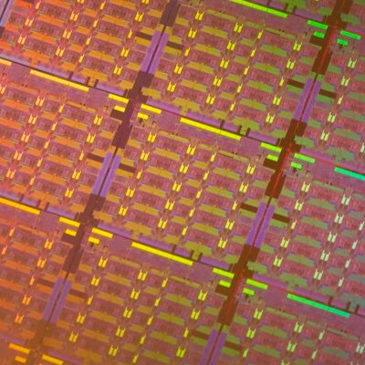
JMS2025での部品・機械器具部門編。 デンソーブースでのパワー半導体の作り方。 RTのウエハーから切り出した半導体チップを電力変換モジュール「パワーカード」に組み込みインバータに搭載。 前工程から後工程、そしてパワエレシステムまでを一気通貫で開発できるのが、デンソーの強み。

JMS2025での部品・機械器具部門編。 デンソーブースでのパワー半導体の作り方。 RTのSiCウエハーに繰り返し微細加工を施し、動作するように仕上げ。 馴染みのあるパワー半導体チップが見えてくる。
0
5
61

🇹🇼TSMCの優秀サプライヤーリスト ※表彰回数:2006年〜2025年(全25回) ・米アプライドは計17回表彰(直近16回連続) ・日本勢トップはSUMCOの計16回(直近12回連続) ・東京エレクが外れたのは2018年以来 ・荏原は2019年以来の表彰 ・表外の日本勢では旭化成、キヤノン、村田機械が2年連続表彰

TSMC 優秀サプライヤーリスト発表 東京エレクトロンは外れる 順位は、アドバンテスト、万潤、アプライドマテリアルズ、旭化成、ASML、オースティンコマーシャル、キヤノン、長春石油化学、中国鋼鉄構造、志勝、ディスコハイテクノロジー、荏原製作所、毓珠建設、建哲精密、J&A、KLA-Tex、KOKUSAI
3
117
741
TSMCのCoWoSに使われる半導体パッケージ基板の価格はいくらぐらいするものなんでしょう。調べても全く出てこない。(調べてすぐ出てきても問題ですが。)
0
0
2
TSMC on HBM4 and C-HBM4E HBM4: - N12 base die - 0.8 V Vdd C-HBM4E: - N3P base die - 0.75 V Vdd - memory controller inside base die https://t.co/YDeSaCEQdl
0
11
86


12月のセミコンジャパン、出展一覧やセミナー詳細等の情報色々出てきましたが。 前から動向追いかけていたキオクシアのDRAMネタが!? 気になるので有給取る準備しておきますかね? https://t.co/na6AB1wkWp
4
8
63

Samsung, SK, and LG All Jump into Glass Substrates… Concerns That “More Investment Validation Is Needed” Remain The electronics affiliates of major domestic conglomerates such as Samsung, SK, and LG are rushing into the next-generation semiconductor glass core substrate market.
6
16
139

あ、ビッグサイトだ。そういやセミコンもう1ヶ月後ですやん?

sn5100触って分かったこと 民生向けNANDはキオクシアがわけわからん強さしてる CMOS直接接合ってそんなに強いんだな・・・ ちなみに直接接合の精度は「直径1kmと仮定して1mm未満が要求される」そうでまさに神業
0
6
64
Microsoft Cobalt 200 - TSMC 3 nm - two chiplets with custom HB interconnect - 132 cores (Armv9.2), 66 per chiplet - 3 MB private L2$ - 192 MB L3$ - 12 memory channels - per core DVFS https://t.co/ZGaykBSOv0
8
46
312

SK Hynix will build four large-scale semiconductor fabs over 3-years at its main Yongin campus in South Korea, investments that could rise to ₩600 trillion won (US$414 billion). to meet growing AI demand, media report, citing SK Group Chairman Tae-won Chey, who announced the SK
koreaherald.com
South Korean conglomerate SK Group said Sunday it will invest 128 trillion won ($87.9 billion) through 2028 in the domestic market, with a focus on chip manufac
3
41
244

Intel’s ‘Advanced Packaging’ Attracts Attention From Apple and Qualcomm, Potentially Opening a New Frontier for the Foundry Business https://t.co/BRxa8j28vr
https://t.co/BRxa8j28vr
wccftech.com
Intel might have been lagging behind in the chip business, but when it comes to advanced packaging, the firm has competitive options.
2
21
140
Samsung unveils first 2nm results… enters the main game in leading-edge foundry Samsung Electronics has officially disclosed the mass production results of its 2-nanometer (nm, one billionth of a meter) process for the first time. As the results of the 2nm node, seen as a
39
133
911