
Ed Sperling
@Chip_Insider
Followers
6K
Following
942
Media
1K
Statuses
6K
Editor In Chief of Semiconductor Engineering #semiconductor #semiEDA #AI #embedded #verification #lowpower #test #DataAnalytics #automotive #ICmanufacturing #ML
Silicon Valley
Joined April 2013
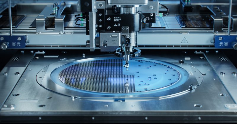
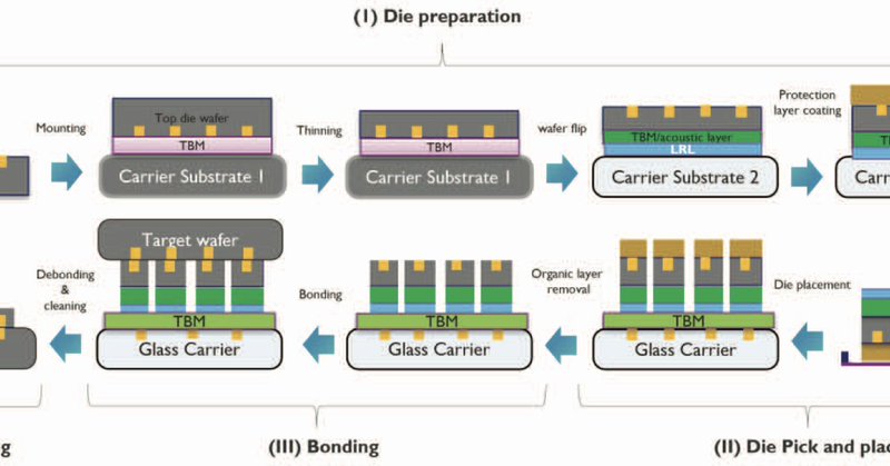
IC Manufacturing At The Limits:.Sub-micron hybrid bonding is set to change how chips are made, but challenges remain. #semiconductor #hybridbonding #2nm #3nm.
semiengineering.com
Sub-micron hybrid bonding is set to change how chips are made, but challenges remain.
0
0
1
Advanced Part Average Testing For Chips:.Unique designs and multi-die assemblies are forcing innovations at the leading edge of testing. #semiconductor #semiconductortest #PAT #PartAverageTesting @yieldWerx #yield.
semiengineering.com
Unique designs and multi-die assemblies are forcing innovations at the leading edge of testing.
0
0
3

How Semiconductor Fabs Use Water:.Water usage at scale requires sophisticated closed-loop systems, digital twins, and multiple filtration strategies, but can water keep up with demand?. #semiconductor #sustainability #water.

semiengineering.com
Water usage at scale requires sophisticated closed-loop systems, digital twins, and multiple filtration strategies, but can water keep up with demand?
0
4
5
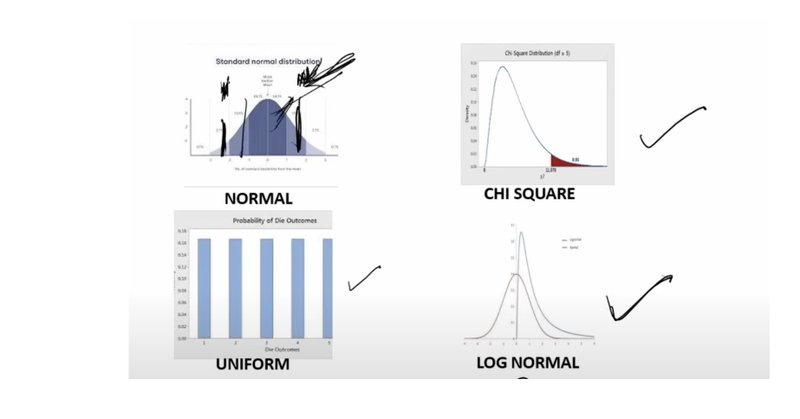
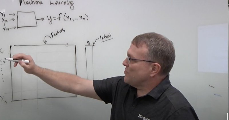
Machine Learning In Semiconductor Manufacturing:.How advances and limitations are defined by the data. #semiconductor #AI @TignisInc #machinelearning #semiconductormanufacturing.
semiengineering.com
How advances and limitations are defined by the data.
1
2
8
News: HW weaknesses; Intel lifelines; EU firms up chip deal; pros/cons of AI chip exports to China; 95% failure in GenAI pilots; Air Liquide’s $3.3B buy; DeepSeek’s latest; Ultra Ethernet; optical semi expansion; imec’s hybrid bonding &. #technology #AI.

semiengineering.com
Intel lifelines; EU firms up chip deal; pros/cons of AI chip exports to China; HW weakness report; 95% failure in GenAI pilots; Air Liquide's $3.3B buy; Taiwan's silicon shield erosion; DeepSeek's...
0
2
9
Latest: EU firms up chip deal; pros/cons of AI chip exports to China; Intel lifelines; HW weaknesses; 95% failure in GenAI pilots; Air Liquide’s $3.3B buy; DeepSeek’s new release; Ultra Ethernet; imec’s front/backside wafer connectivity & . #semiconductor.
semiengineering.com
Intel lifelines; EU firms up chip deal; pros/cons of AI chip exports to China; HW weakness report; 95% failure in GenAI pilots; Air Liquide's $3.3B buy; Taiwan's silicon shield erosion; DeepSeek's...
0
1
7
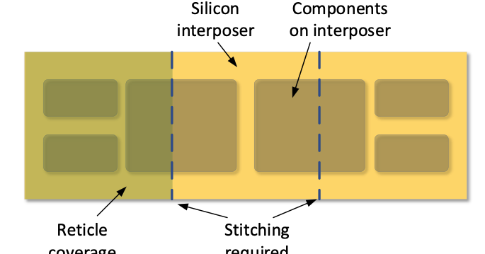
Adv. packaging often relies on silicon interposers to connect chiplets & other components inside a package. The problem is that interposers typically exceed the reticle limit, which adds both complexity & cost. #semiconductor #interposer #interconnects.
semiengineering.com
Scanner improvements, bridges, and panels may bring relief.
0
2
7
RT @SemiEngineering: New technical papers recently added to Semiconductor Engineering’s library. #semiconductor #ph….
0
3
0
Workload-Specific Hardware Accelerators:.What differentiates accelerators from other processing elements. #AI #NPUs @expedera #hardwareaccelerators.
0
2
11
RT @SemiEngineering: Diversity of compute elements proliferates for inferencing, depending on application space. #….
semiengineering.com
Diversity of compute elements proliferates for inference, but the mix varies by application.
0
1
0
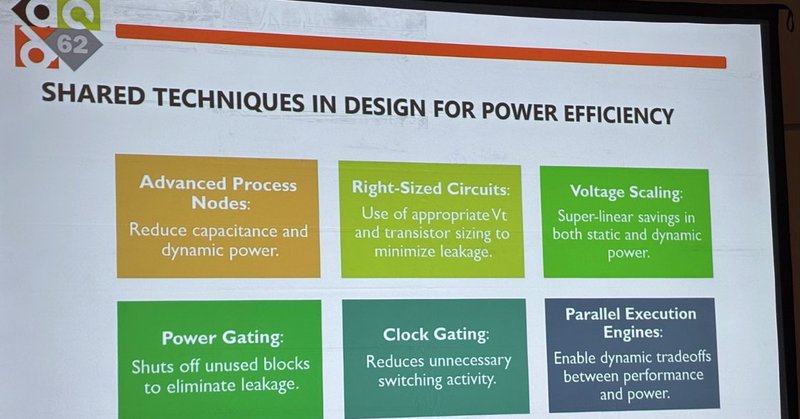
RT @SemiEngineering: Re-Architecting AI For Power:.Is AI using too much power? Some people think so, and believe the easy gains in power re….
semiengineering.com
Is AI using too much power? Some people think so, and believe the easy gains in power reduction have already been made.
0
5
0
What’s Different About HBM4.New DRAM standard aims to solve a critical bottleneck. #HBM #DRAM #HBM4 #memorybandwidth #datacenter #AI #LLMs

1
6
22
RT @Chip_Insider: Shrinking interconnects expose limitations in traditional inspection methods, forcing new approaches to overlay, surface….
semiengineering.com
Shrinking interconnects expose limitations in traditional inspection methods, forcing new approaches to overlay, surface quality, and defect detection.
0
4
0
Security issues may be magnified by the number of agents and their potential interactions, not all of which may be obvious to chipmakers. #AgenticAI #semiEDA #cybersecurity #chipdesign

0
1
4
Latest: US stake in Intel?; 15% pay-for-play on chip sales; neural-accelerated GPUs; critical minerals funding; $1.8B acquisition; thermodynamic chip; new crypto standard; lawsuit and IP theft; dynamic power analysis app; Ansys-NVIDIA deal..#semiconductor.
semiengineering.com
US stake in Intel?; 15% pay-for-play tax on chip sales; Arm's neural-accelerated GPUs; critical minerals funding; $1.8B acquisition; thermodynamic chip; new crypto standard; lawsuit and IP theft;...
0
3
7
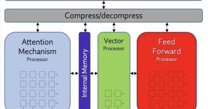
New approaches are needed as current processors run out of steam. #processors #chiparchitecture #semiEDA #EnergyEfficiency.
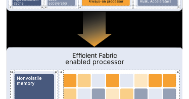
semiengineering.com
New approaches are needed as current processors run out of steam.
0
3
5

Shrinking interconnects expose limitations in traditional inspection methods, forcing new approaches to overlay, surface quality, and defect detection. #semiconductor #hybridbonding #metrology.
semiengineering.com
Shrinking interconnects expose limitations in traditional inspection methods, forcing new approaches to overlay, surface quality, and defect detection.
1
4
8
Advancements in vehicle architectures, AI, and security are reshaping the future of the car. #SDVs #AutonomousDriving #automotive.

semiengineering.com
Advancements in vehicle architectures, AI, and security are reshaping the future of the car.
0
4
5
RT @Chip_Insider: Every aspect of data center energy use must be optimized to reduce power consumption and enable more sustainability, from….
semiengineering.com
Every aspect of data center energy use must be optimized to reduce power consumption and enable more sustainability, from chips to transformers and edge compute.
0
5
0