

Semiconductor Engineering
@SemiEngineering
Followers
16K
Following
876
Media
1K
Statuses
7K
Deep Insights For The Tech Industry #semiconductor #semiEDA #AI #embedded #verification #lowpower #test #DataAnalytics #automotive #chipdesign #ICmanufacturing
Silicon Valley
Joined September 2013
Latest: IEDM blitz; Arteris’ security buy; RISC-V acq.; photonics deals; Nvidia H200 to China; 1.4nm patterning; standard package HBM; earnings; US rare earths surprise; $475M analog AI chip $; PCIe security warning https://t.co/nc02NEAOj9
#semiconductor #technology #AI #semiEDA
semiengineering.com
IEDM announcement blitz; Arteris' security buy; Qualcomm's RISC-V acquisition; UMC photonics; Nvidia H200 to China; 1.4nm patterning; standard package HBM; earnings; US rare earths surprise; $475M...
2
5
7
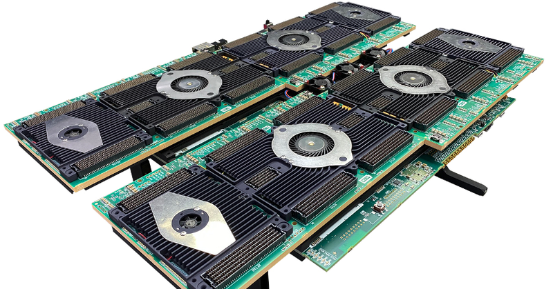
Chiplets serve a similar function as the soft IP widely used in chips today, but the similarities end there. https://t.co/IusApWPCWj
#chiplets #SoftIP #RTL #semiconductor
0
0
6
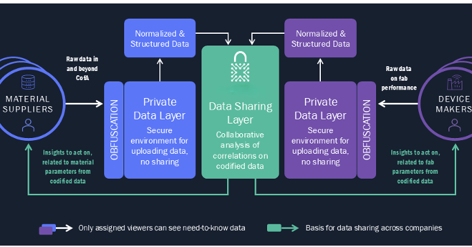
Real-time security clearances are becoming increasingly common in manufacturing of advanced-node semiconductors, where data sharing is both essential and a potential security threat. https://t.co/ONjXPSoOFB
#semiconductor #ZTAs #ZeroTrustARchitectures
#semiconductormanufacturing
semiengineering.com
Collaboration becomes necessary at advanced nodes, but implementation can be painful.
1
1
4
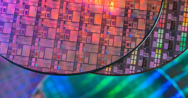
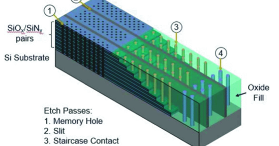
Metrology Digs Deep To Produce Next-Gen 3D NAND: Deep vertical holes and re-entrant features challenge the best metrology methods. https://t.co/AOI7kwAfZC
#semiconductor #3DNAND #metrology #IRCD #inspection
semiengineering.com
Deep vertical holes and re-entrant features challenge the best metrology methods.
1
2
7
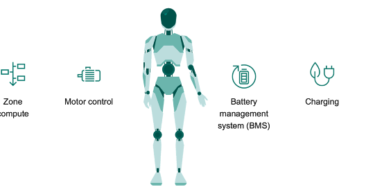
Robots are becoming smarter, more capable, & more pervasive, setting the stage for a whole new round of growth that will touch nearly every part of the semiconductor and software industries for decades to come. https://t.co/FRLUb7p4xu
#edgeAI #PhysicalAI #robots #functionalsafety
semiengineering.com
The automotive industry has established safety standards, but rules concerning safety-critical physical AI are still evolving as more robots work alongside humans.
2
5
7
A new technical paper “AI for quantum computing” was published by researchers at NVIDIA, University of Oxford, University of Toronto, Quantum Motion, University of Waterloo et al. https://t.co/TtALU8MtTp
#quantumcomputing @nvidia @UniofOxford @UofT #AI @QuantumMotion @UWaterloo

semiengineering.com
A new technical paper “Artificial intelligence for quantum computing” was published by researchers at NVIDIA, University of Oxford, University of Toronto, Quantum Motion, University of Waterloo et...
0
4
5
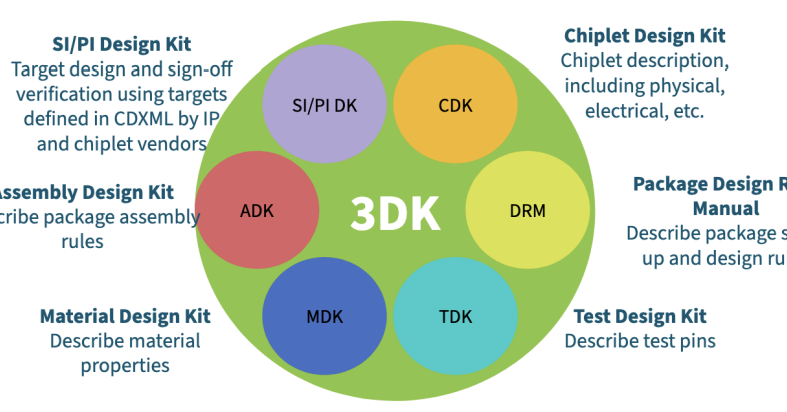
Validating design kits requires investment and collaboration across the supply chain, but it pays off in fewer layout respins and lower risk. https://t.co/57CDzFkTmi
#chiplets
semiengineering.com
Validating design kits requires investment and collaboration across the supply chain, but it pays off in fewer layout respins and lower risk.
1
3
6
Latest: 3D printed chip packages; UMC-Polar; US stake in EUV litho; Micron exits biz; Canada invests in IC packaging; new thin films site; GaN deal; chiplet challenges, benefits; FeFETs for low-power NAND flash; Marvell's buy... https://t.co/TTbpg7xqF6
#semiconductor #semiEDA
semiengineering.com
3D printed chip packages; UMC-Polar deal; Marvell's photonics acquisition; US stake in EUV litho; global IC forecast raised; Micron exits consumer biz; Canada invests in IC packaging; new thin films...
1
7
11
New technical papers recently added to Semiconductor Engineering’s library https://t.co/17slU6X5gQ
#semiconductor #chiplets #neuromorphic #semiEDA
#NSFETs #IMC #verification #VLSI #hardwaresecurity
0
1
5
Latest: 3D printed chip packages; UMC-Polar; US stake in EUV litho; Micron exits biz; Canada invests in IC packaging; new thin films site; GaN deal; chiplet challenges, benefits; FeFETs for low-power NAND flash; Marvell's buy... https://t.co/TTbpg7xqF6
#semiconductor #semiEDA
semiengineering.com
3D printed chip packages; UMC-Polar deal; Marvell's photonics acquisition; US stake in EUV litho; global IC forecast raised; Micron exits consumer biz; Canada invests in IC packaging; new thin films...
1
7
11
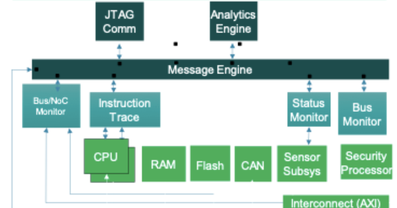
Special Report: Real-time monitoring and proactive risk mitigation can identify vulnerabilities and attacks throughout a device’s lifetime, and much more. https://t.co/IufkE1gGOC
#hardwaresecurity #SLM #SiliconLifecycleManagement #semiconductor #semiEDA
semiengineering.com
Real-time monitoring and proactive risk mitigation can identify vulnerabilities and attacks throughout a device's lifetime, and much more.
0
1
3
Optimizing AI Workloads For Edge Computing: Performance enhancement, cost reduction, data security, and improved energy efficiency are the end goals for optimizing AI workloads at the edge. https://t.co/LBSbwqGAUS
#EdgeAI #AIworkloads #edgecomputing #LLMs
1
2
3
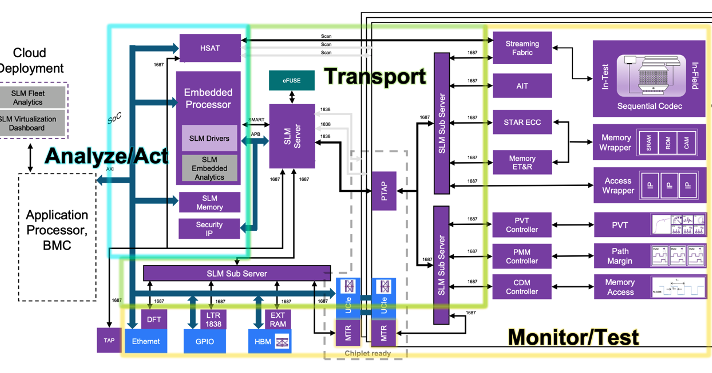
Designing resilient chips with SLM can help combat aging effects, security threats, and get to market faster with higher yields. https://t.co/WOfyY0eAXb
#SLM #SiliconLifecycleManagement #semiEDA #chiparchitectures
semiengineering.com
Designing resilient chips with SLM can help combat aging effects, security threats, and get to market faster with higher yields.
1
3
10
Validating design kits requires investment and collaboration across the supply chain, but it pays off in fewer layout respins and lower risk. https://t.co/57CDzFkTmi
#chiplets
semiengineering.com
Validating design kits requires investment and collaboration across the supply chain, but it pays off in fewer layout respins and lower risk.
1
3
6
Breaking news: Nvidia and Synopsys announced a multi-faceted, multi-year deal that includes everything from digital twins to CUDA programming, engineering, and marketing collaboration, and Nvidia’s $2B purchase of Synopsys stock. https://t.co/JdJpJeHJTd
0
6
12
Latest: China’s DDR5/LPDDR5X; government fundings climb; GF’s latest deal; Rapidus $; GPU vs. TPU; TSMC’s 2nm fabs; ASIC acquisition; diamond chip foundry; data sharing in IC manufacturing; how Americans use AI; open-source chiplets ... https://t.co/JdJpJeHJTd
#semiconductor

semiengineering.com
Nvidia's $2B investment in Synopsys, plus multi-year collaboration; Micron's new HBM plant; China's DDR5/LPDDR5X; global government fundings climb; GF's latest photonics deal; Rapidus' infusion; GPU...
0
7
10
New technical papers recently added to Semiconductor Engineering’s library https://t.co/CmmZd1H1fb
#semiconductor #interconnects #DRAM #chiplets #accelerators #CFET #NSFET
0
2
9
The application of AI into design tools and flows will take several forms, each independent, but all potentially working together. https://t.co/3GzrKQh8Dr
#semiEDA #AI #chipdesign #AgenticAI #semiconductor #verification

semiengineering.com
The application of AI into design tools and flows will take several forms, each independent, but all potentially working together.
0
4
6
Latest: China’s DDR5/LPDDR5X; government fundings climb; GF’s latest deal; Rapidus $; GPU vs. TPU; TSMC’s 2nm fabs; ASIC acquisition; diamond chip foundry; data sharing in IC manufacturing; how Americans use AI; open-source chiplets ... https://t.co/JdJpJeHJTd
#semiconductor
semiengineering.com
Nvidia's $2B investment in Synopsys, plus multi-year collaboration; Micron's new HBM plant; China's DDR5/LPDDR5X; global government fundings climb; GF's latest photonics deal; Rapidus' infusion; GPU...
0
7
10
Growing use cases include life science AI, reducing memory and I/O bottlenecks, data prepping, wireless networking, and as insurance for evolving protocols. https://t.co/tH1Ah6HVpM
#FPGA
semiengineering.com
Growing use cases include life science AI, reducing memory and I/O bottlenecks, data prepping, wireless networking, and as insurance for evolving protocols.
1
1
4