

🌿 lithos
@lithos_graphein
Followers
15K
Following
27K
Media
4K
Statuses
14K
Semiconductors - Follow me to learn all about microchips & how we print them. My web scraper is a live dashboard for the freshest tech news & press releases.
🗽
Joined November 2022
I forgot who it was, but someone on here disagreed with me that it's possible to tell if an SEM image is photoresist or if it's after-etch into a hard mask, like SiN…anything that's not photosensitive. I can tell by the exposure dose of the SEM image. All photoresists are
4
6
76

Apparently we now (for the first time?!) have methods to study the behavior of photoresist in situ, and this can bigly improve yields By *we* I mean China; since it's openly published, it's not some deep IP… I guess. @lithos_graphein @zephyr_z9 @basedjensen is this a big deal?

New Cryo-ET tool offers unprecedented 3D clarity into chip lithography, unlocking cheaper, cleaner manufacturing. https://t.co/IlTgMAgcxI
5
5
87

半導体国際会議参加独自記事掲載しました!)半導体洗浄技術クリーン化技術シンポジウムUCPSS 2025レポート(2) ウェハ乾燥時の高アスペクト比微細パターン倒壊問題が最大の課題 サムスンは世界に先駆け超臨界流体乾燥をDRAMに次いでロジックにも採用 詳しい記事は➡️ https://t.co/CXh4XdHHE3
0
7
81
SemiAnalysis is on a tech meme tear. 😂

Scaling workflows with GitHub Actions has never been more difficult! As we scale InferenceMAX to become one of the world's largest GPU CI/CD fleets, we keep hitting arbitrary platform limits. In particular, there's a 256 job cap per matrix generation, a ~1000 artifact download
0
0
7
Continuous flow polymer synthesis is the holy grail for chemistry right now. For semiconductors it can be used to make polymers for photoresists and BARCs. Brewer lists the generic advantages in their abstract here: • enhanced reaction control • improved reproducibility •
2
3
44
Information exchange on a mass scale. I come from a long line of printers. Same thing different era.

isnt it funny that computer chips are just an extension of print technology
0
1
17
ASML has the best technical marketing team. This video explains in layman's terms how source mask optimization (SMO) works. It's the engineering sorcery behind printing the most advanced chips.
55
540
4K
The field-effect transistor (FET) was patented by Julius Edgar Lilienfeld in 1925, but the patent expired before anyone could figure out how to actually make it.
2
5
55
If you were wondering how something like this works... LAM (Coventor) published a self-aligned litho-etch litho-etch (SALELE) process flow for 18 nm pitch metal in a PR td. It's different from Intel's version published in the journals. This uses low-NA EUV at a relaxed pitch to
4
11
136

Korean semiconductor equipment startup breaks Carl Zeiss’s monopoly, supplies EUV inspection equipment to Japanese photomask company A South Korean semiconductor equipment startup has supplied hundreds of billions of won worth of ultra-precise extreme ultraviolet (EUV) mask
19
144
815
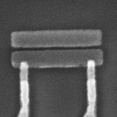
Yes, litho eye sees this. Not normal. How do you print this with a scanner?
13
5
154
Did they publish anything more than 2 SEM images? Lmk

Good lord. Please don’t consume this kind of semiconductor “analysis”. I implore you.
3
0
64
Litho Eye Anomalies: 1) These are etched lines, not trenches. It may indicate it's a negative-tone photoresist system. 2) There is a clear top-to-bottom signature for the lines where the tops are wider and the bottom tails off in width. Or it's the inverse of this. Almost every
16
17
286
Don't spill it on your shoe. It leaves a mark.
one of the chemicals that people often use to remove resist in lithography - NMP - causes infertility from repeated exposure to touching it. and it goes through gloves btw
3
0
30
Can't fool the litho eye. Do you see the trick here?

6
0
33
How's that sanctions-busting immersion scanner coming along?
4
2
39
But 🇺🇸 Tesla has awesome EVs, it's so simple and inevitable in coming years. "Building such a unique supply ecosystem requires decades of effort plus billions of dollars in annual capital expenditure. OSAT margins are slim, so starting anew elsewhere yields nearly zero return
1
0
25
EUV in the wild. Looks like we have a step stool there for manually loading the reticle pods.

Intel's $INTC CEO just revealed its Panther Lake architecture, and the first thing he did was take a picture next to an $ASML EUV lithography system.
4
9
112

ASML 스캐너의 역사 와 중국의 도전 (25.10.24) The History of ASML Scanners and China's Challenges (October 24, 2025) {blog post summary of @lithos_graphein's thread) https://t.co/iZQ9OMAl5C

spedtrder.tistory.com
들어가며...칩 프린터 (리소그래피 장비) 를 통해 AI 혁명을 실현하고 있으며 이는 지금까지 만들어진 기계 중 가장 복잡한 기계입니다. The List - ASML 스캐너 목록지난 35년 동안 설치된 모든 ASML 스캐너 모델 목록을 소개합니다. 완전한 목록은 아닙니다. 몇 가지 빠진 것도 있을 수 있지만, 제가 직접 사용해 본 도구(대부분...
2
1
7