

Jonas Sundqvist 🐳
@jv3sund
Followers
1K
Following
12K
Media
4K
Statuses
16K
CEO of AlixLabs and BALD Engineering. Atomic Layer Deposition -ALD, Precursors & Electronic Specialty Gases. Based in Dresden, Germany, #ALDep #CVDep #ALEtch
Dresden, Sachsen
Joined December 2010
RT @Applied4Tech: Today we reported results for the third quarter of fiscal 2025. Check out this snapshot to learn more about our financial….
0
2
0
RT @F_Boesenberg: Chipfertigung in Deutschland: #ESMC-Chef Dr. Christian Koitzsch im Interview | heise online
heise.de
Wir hatten die Gelegenheit, mit dem Chef von TSMCs erster europäischer Niederlassung zu sprechen: ESMC-Präsident Dr. Christian Koitzsch.
0
3
0
Now Pitching for more Sustainable Semiconductor Processing. Off -Grid. Not sharing my MS Teams foreground

1
0
2
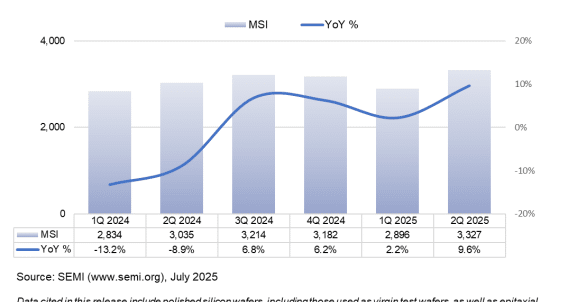
RT @SEMIconex: According to our latest quarterly analysis, worldwide silicon wafer shipments reached 3,327 million square inches in Q2 2025….
0
3
0
RT @trendforce: #Samsung Electronics Q2 Revenue Reaches ₩74.6T – Memory Demand Strong, But Margins Weakened by Costs. Samsung Electronics h….
0
2
0
RT @Semi_Dig: SEMI Reports Worldwide Silicon Wafer Shipments Increase 10% Year-on-Year in Q2 2025 - #semiconductord….
semiconductor-digest.com
The SEMI Silicon Manufacturers Group reported that worldwide silicon wafer shipments increased 9.6% year-on-year to 3,327 million square inches (MSI) from the 3,035 MSI recorded during the same...
0
2
0
RT @TweetTrymax: Full speed ahead richting Amerikaanse, Aziatische en Europese markt: #semiconductors #globalexpan….
0
1
0
RT @crmiller1: How is it that, despite our reliance on chips produced in Asia, America runs a sizable trade surplus in semiconductors? I ex….
aei.org
The US should focus tariffs on Chinese-made chips while striking sectoral trade deals with allies that commit both sides to zero tariffs, reducing nontariff barriers, and continuing to invest in...
0
7
0
RT @F_Boesenberg: Globalfoundries will CPU-Urgestein MIPS Technologies übernehmen | heise online
heise.de
Der Chipauftragsfertiger Globalfoundries will sein eigenes IP-Portfolio erweitern. Dazu steht ein Kauf von MIPS Technologies an.
0
1
0
No EUV? No problem! @AlixLabs.
“Swedish startup Alixlabs is preparing for commercial deployment of a new semiconductor patterning technique that unlocks leading-edge semiconductor manufacturing without the need for EUV.”.
1
0
3
RT @F_Boesenberg: #ESMC building site in #Dresden, the two finished buildings are the Bosch Fab and the Mask House #AMTC (JV between Global….
0
5
0
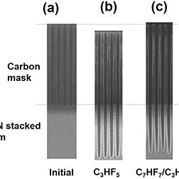
RT @JVSTAB: To meet growing storage capacity demands, researchers from Kioxia propose the use of fluorocarbon gas as an etchant in 3D flash….
pubs.aip.org
In the high-aspect-ratio hole etching process, there is a strong need for high selectivity of SiO2 and SiN films against the amorphous carbon mask. To meet this
0
1
0
RT @EU_Startups: Build, scale, impact: Applications for the Amazon Sustainability Accelerator 2025 are now open! . Apply today and scale yo….
eu-startups.com
Are you a sustainable startup looking to maximise your impact? The Amazon Sustainability Accelerator is now open for applications, offering ambitious
0
3
0
RT @SEMIconex: SEMI’s Latest 300mm Fab Outlook Report Is Out Now! . With insights spanning memory, logic, foundry, and more, this report is….
0
3
0
RT @Jukanlosreve: AWS and AMD are reportedly moving up the timeline for adopting glass substrates in an effort to compete with Nvidia. htt….
ebn.co.kr
글로벌 빅테크와 유리기판 퀄테스트를 진행 중인 SKC가 생산능력을 최대 10배로 늘리는 투자안을 검토하고 있는 것으로 나타났다. 관건은 최종 고객사의 승인과 자금
0
16
0
RT @trendforce: 💥With #TSMC and #Intel charging toward 2nm and 18A in 2H25, #Samsung is reportedly taking a more grounded route—doubling do….
0
1
0