
Massive PCB Technologies
@MassivePcb
Followers
925
Following
42
Media
33
Statuses
44
#Multilayer #PCB, #quickturn #prototype, #rigidflex, #FPC, #HDI #smallvolume #Rogers, #Taconic... and #PCBA / [email protected]
Hongkong
Joined October 2019
High-density interconnect (HDI) boards came into being and became the first choice for high-end electronic products. What are the differences between HDI boards and ordinary PCBs?.
linkedin.com
The major differences between HDI boards and ordinary PCBs Basically, HDI is a high-density circuit board that uses micro-blind buried via technology, and its line distribution density is much higher...
0
0
0

Turn old photos into videos and see friends and family come to life. Try Grok Imagine, free for a limited time.
702
1K
5K
Hey there!.Production is running well,how's going on with your next project?#Multilayerpcb #FPC #Rigidflex #PCBsolution #PCBassembly #HDIboard #Hightechpcb
0
0
1
MASSIVE PCB wish all of you Merry Christmas and a happy 2025!.May you be filled with love,joy,health and success in this new year!
0
0
1
Interposer PCB is now being widely used in high-performance computing, artificial intelligence, data centers, communications and other fields. Below is a 24L 6steps Anylayer HDI PCBs which is one of our high-precision circuit boards.

1
0
1
Thick copper PCB has gradually become an important trend in the electronics field due to its unique material properties. Below is one of thick copper PCBs which produced by us,it is a 4L board,and the copper is 10/3/3/10OZ.

0
0
1
Our loved PCBs began in 1930s with Austrian engineer Paul Eisler. By etching conductive pathways onto an insulating board, Eisler revolutionized electronic circuits, making them more compact and reliable. At MASSIVE, we continue Eisler's legacy of innovation.

0
0
1
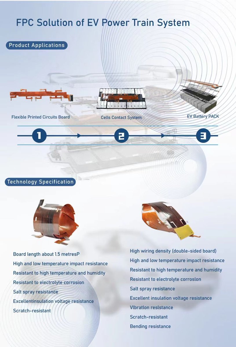
Ultra large Size Flexible Printed Circuits Boards For Cell Contact System Of EV Battery Pack. If you're interest in this technology,feel free to contact us through info@massive-pcb.com.
0
0
2
Our team of MASSIVE PCB deeply appreciate you,our valued customers,being an essential part of our successes.May this day be filled with warmth,joy,and the company of loved ones. Happy Thanksgiving!
0
0
2
We have brought in a new machine this month,which is used for adding stiffener automatically on FPC.Mostly this process is done by manually which with high labor costs and low precision,now we have this machine.All we've done is for lower cost and better quality to you!
0
0
1
Chinese National Day is coming soon,MASSIVE will provide QTA(Quick Turn Around)services to catch customers' production planns before the holiday.
0
0
1
✔4 Steps HDI.Material:FR4 High TG、High-speed material.Stack up:Multi-step stacked.Width / Space:50um/62.5um.Impedance tolerance:±10%.Multi-layer buried & blind hole design.Partially plating hard gold #MASSIVEPCB #pcb #pcbassembly #printedcircuitboard #pcbmanufacturer

0
0
1
There is really no limit to the number of layers that can be fabricated in a multilayer PCB. In this pdf file, you can see the most common 7 kinds of multilayer PCB configurations.

0
0
1
With over 10 years' experience of PCB solutions provider,we can be very supportive for your products,whatever on the process design or the cost-effective ways of fulfilling your strategic project management.Let's grow with you very fastly!

0
0
2


Unlike normal PCB (rigid board), FPC can bend, fold or repeat motion in many ways. Check out our design guide focusing on the design and manufacturing of FPC,and send your queries to us through info@massive-pcb.com.
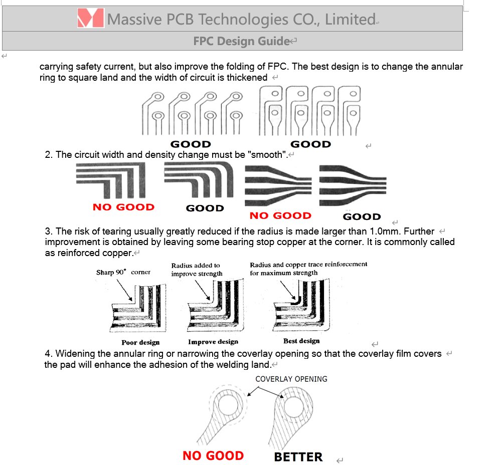
1
1
3
MASSIVE PCB wishing you and your family a happy,healthy and fantastic 2022!. Waiting for snowflakes, Christmas trees, new year fireworks, and. better us!
1
0
2
Below area is only 0.25mm,routing only on 2 internal layers layer 3 &4 in this area.(6L board.)We used two times depth control milling by laser before ENIG on front and back side. Do it as step board instead of rigid-flex to help customer saving costs greatly.

1
0
5
Below is one of special boards recently supplied by us,we aim to supply the best minds. Mixed Dielectric PCB.12L Rogers 4350B+FR4 TG170.Mixed copper H/H/H/H/1/1/H/H/H/H.Board thickness: 1.37+/-10%mm.Min trace width/gap: 3.5mil/3.5mil

0
1
6